PCB Fabrication
PCB fabrication is short for printed circuit board fabrication, it is the complete manufacturing process of realising a design with circuit patterns into a physical and functional PCB bare board.
What is PCB Fabrication?
PCBs can be categorised into single-layer PCB, double-layer PCB, multilayer PCB, rigid PCB, flexible PCB and rigid-flex PCB usually. Different kind of PCB has different fabrication processes and techniques, but generally speaking, PCB fabrication includes the following processes: base material cutting, drilling, plating, copper trace etching, solder mask printing, silkscreen printing, surface treatment, E-testing, PCB components placement, functional testing and visual inspections.
Our PCB Fabrication Capabilities
PCB TYPES:
Rigid, Flex, Rigid-flex, Semi-flex, HDI, RF & microwave, IC Substrate
PCB Materials:
FR4, Polyimide, Kapton, PET, Aluminum-based, Copper-based, Metal-based, Alumina Ceramic, Ceramic, Hybrid material, Halogen free, High Speed, High frequency, PTFE, Teflon
Technologies:
Blind vias, Buried vias, VIPPO, Conductive via plug, Non-conductive via plug, Backdrill, impedance control, Heavy copper, Gold fingers, Embedded
Layer Counts:
1-40 layers for mass production, upto 100 layers for prototyping
Thickness & Dimensions:
PCB Thickness: 0.10-10.0mm
Max. PCB Dimensions: 1500x508mm
Surface Finishes:
HASL, OSP, ENIG, ENEPIG, Immersion Silver, Immersion tin, Gold Connector, Selective hybrid finishes.
Why Choose Rush as your PCB Fabrication Partner
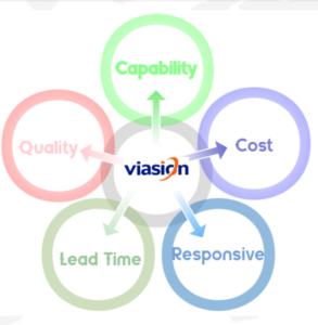
Competitive Pricing:
With our 16+ years of experience in PCB fabrication, we have built a strong engineering, production and purchasing team, which helps us to ensure we can supply printed circuit boards at the lowest possible price and high quality.
High Quality and International Standards:
All our PCBs are produced and inspected according the internal standards, such as IPC-A-600, IPC-A-610 and UL (E358677) standards. The production facility strictly follows ISO9001 and ISO13485 to make sure our PCBs are produced at the highest quality.
Experience Engineering and Production Team:
We have been supplying printed circuit boards since 2007. Our engineering and production team know all kinds of PCBs very well. We know all aspects of PCBs, including base material, DFM, production, testing, inspection, failure analysis., etc.
Reliable and Responsive:
Many customers trusted us for more than 10 years. This is because we always supply good quality products. Our dedicated customer service team always reply our customers on time, no matter if it is RFQ and order, or complaints and pull-in of delivery date.
One-stop Solution:
We supply a wide range of PCBs, including standard rigid PCB, flexible PCB, rigid-flex PCB, HDI PCB, high-speed PCB, high-frequency PCB, Teflon PCB, IC PCB, embedded PCB…Besides, we can also supply a one-stop service for PCB fabrication and PCB assembly. So you can rely on us to meet your PCB demands.
Quick Lead Team:
Our standard lead time for PCB fabrication is 1-4 weeks, depending on the layer, material, techniques, and quantity. But we can also supply quick-turn PCBs in 24 hours. Please contact us for any of your PCB requirements.
Common Types of PCB Fabrication
The classification of PCB boards is hard to define. However, the most common is number of layers and substrate used.
(1) number of layers: single-sided PCB, double-sided PCB and multi-layer PCB;
(2) substrate used: rigid PCB, flexible PCB, and rigid-flexible PCB.
Single-sided PCB:
Single-sided PCB is the least cost and simplest PCB type made with one layer of copper on one side. Electrical components are also populated on one side only. The low cost is due to simple PCB fabrication services and few components.
Double-sided PCB:
A double-sided PCB is a kind of circuit board with two copper layers, which are the top copper layer and the bottom copper layer. The top copper layer and bottom copper layers are connected by through-holes.
Multi-layer PCB:
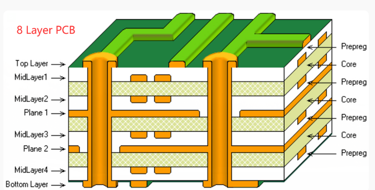
As the name suggests, a multi-layer PCB consists of several working layers, with the top layer acting as the surface for component placement while the bottom layer for routing and welding. The layers in-between have multiple functions like signal, conductor, and grounding. Multi-layer PCBs consist of vias which are vertical structures that connect traces on each layer. Fabricating PCB with several layers starts with preparation of the FR-4 copper-clad laminate and the prepreg sheets.
Rigid PCB:
Rigid PCBs are printed circuit boards made of rigid materials, such as FR4, Metal core, ceramic, alumina., etc. Rigid PCBs cannot be bent, but they supply good support to the assembly of electronic components. Rigid PCBs are widely used in almost every industrial area and are the most commonly used circuit boards.
Flexible PCB:
Flexible PCBs are beneficial in miniaturizing devices. This type of PCB has wide broad applications in various fields, including cameras, mobile phones and RFID cards. Surface-mount technology can also be applied in fabricating PCB of this kind. Special types of fixtures are required to hold flexible PCB during reflow soldering. Flexible PCB has different material properties like density, specific heat capacity and thermal conductivity.
Rigid-flex PCB:
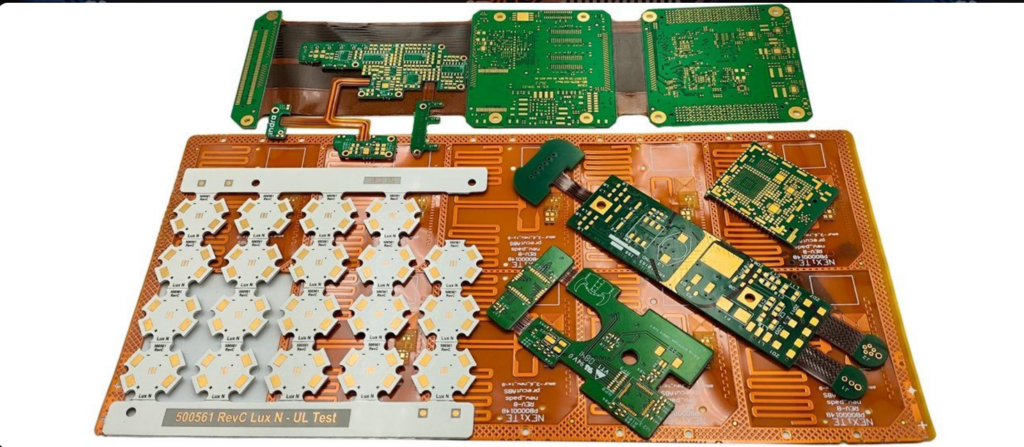
Rigid flex PCBs combine rigid and flexible materials together, to have the advantages of both rigid PCB and flex PCBs. Components are always assembled on rigid parts since we can route high-density drills and wires on rigid parts; flexible parts are usually used to connect the rigid parts and they can be bent or twisted to different shapes.
Flexible parts are usually produced from polyimide material, which has excellent flexibility, heat resistance and machining performance.
So rigid-flex circuit boards are normally used on high-tech electronic products, such as smartphones, laptops, digital cameras, robotics., etc.
Applications of PCB Fabrication
Printed circuit boards have wide applications in various fields, such as industrial, medial, automotive, telecommunications, robotics, energy and power, test and measurement, and aerospace., etc., Below are just several common fields that PCB fabricators focus on:
Consumer Electronics:
This is the most used type of application intended for entertainment and information. Typical examples include mobile phones, laptop, television, etc. Printed circuit board fabrication adjusts to diversified needs as more features are being introduced in the electronic devices.
Automation and Control:
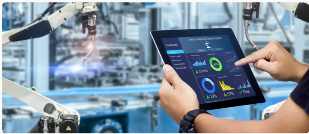
With the development of new technology, automatical equipment is widely used in many industrial areas, such as agriculture, industrial control systems, robots, IoTs., etc. This kind of PCB usually consists of a multilayer circuit board with more than 4 layers, some of them may need high layers or HDI PCBs.
Power & Energy:
Almost all electronics need a power PCB, which is used to supply electricity and achieve functions. With the development of new energy, especially EVs, and UPS power suppliers, more and more PCBs are required in this industrial. This kind of PCB always needs high TG 170 or above material, thick copper may be needed, from 2oz to 10oz normally.
Automotive:
Reliability and quality are critical in this type of application as it is directly related to people’s lives. Printed circuit boards are often involved in manufacturing automotive cameras and pressure and motion sensors for airbag launchers. The high requirements of the automotive industry drive PCB fabricator to have rigorous controls and stringent reliability tests in compliance with automotive standards.
Medical:
Since medical equipment requires utmost care and precision, PCBs are used to control these specific functions. Some of medical devices include pacemakers, blood pressure monitors, implants, and handheld monitors. It is also important to abide by the regulatory requirements for medical applications.
Basic Materials in PCB Fabrication
In this section, we will discuss various materials and layers that help us fabricate PCB boards.
Dielectric Substrate Material:
The material that is sandwiched between the copper layers is known as dielectric material. This material can further be divided into core and prepreg. As mentioned earlier, the most commonly used dielectric material is FR4 which means resin impregnated woven glass fabric. Most PCB fabricators use FR-4 as a default substrate material.
Solder Mask:
The solder mask primarily serves as protection of the copper layer from corrosion due to exposure to outside environment. The solder mask also guides the solder along the copper pad.
core:
A core consists of two copper foil sheets with an insulating layer in between. The copper is used for conductivity while the insulating layer is used for mechanical support and electrical insulation.
Prepreg:
Prepreg is frequently mentioned in PCB board fabrication. For multi-layer PCB, several cores can be joined together. This is the specific purpose of prepreg, but unlike the core, prepreg is softer and more pliable. It is made of an uncured resin and a glass weave. The PCB fabricators put the prepreg between the core layers and under a defined temperature and pressure, and the prepreg will bind the cores together. The core and prepreg are almost undistinguishable after this curing process
Copper Foil:
Copper traces and pads are drawn on each layer using a layout tool, but the PCB fabricator actually starts with a complete layer of copper. The copper that is not required in the design is being etched away. The copper pads that are being used for surface mounting still require a surface finish as copper is now easily oxidized
Vias:
As reiterated in the prior sections, the layers are insulated from each other, thus a structure is needed to allow the layers to connect. This is realized by drilling a copper plated hole, allowing connection from one layer to another. There are also various types of vias that depend upon the design and complexity of the device:
Through-hole: The most popular and cheapest method where the vias connect one layer to another.
Blind: Vias connect the top or bottom to the internal layer but does not go through all the layers.
Buried: This via does not extend to the top or bottom layer, because it connects only the internal layers.
Micro via: Very small vias that are drilled through laser, mostly used for small pitch and high-density devices.
The cost of fabricating PCB highly relies on the number of vias due to the additional steps required like drilling and copper plating.
Main steps in PCB Fabrication:

PCB board fabrication is comprised of steps that may vary in reference to design, number of layers and component layout and complexity. Below are the major processes involved in PCB fabricate:
Circuit Design:
To come up with a fully functional circuit, a circuit design must first be generated using a Computer-Aided Design (CAD) software system. The design workflow starts with circuit development, layout definition and CAD program generation. Circuit elements are assigned to different CAD layers based on the intended functions. Furthermore, component placement, trace routing and component package types are detailed in the layout. The objective is to include as many data as possible for reference. From the CAD tool, a generator tool is used to develop control programs for fabricating PCB.
An industry-recognized photo-plotting tool called “Gerber” is being used which is the basis of printed circuit board fabrication equipment to fabricate PCB. A complete set of Gerber files must be sent to the PCB fabricator, with completely generated files for each layer.
Patterning:
The patterning process can be done through ‘photolithography’. In photolithography, a photosensitive material, also known as photoresist, is coated into the copper foil and then exposed to light. During exposure process, a photomask is used to cover the wanted pattern on the printed circuit board fabrication. The exposed portion of the PCB is applied with a solution, dissolving the photosensitive material. Another solution is applied to etch away the soluble photosensitive material along with the unwanted copper foil. The copper foil is then left with the pattern like that of the photomask. Lastly, the residues are stripped through a cleaning solution. The basic flow of PCB board fabrication can be summarized as: exposure, developing, etching, and stripping.
Drilling:
Recall that vias are the structures that connect layers. This is made possible by drilling a hole using mechanical or laser drill. The drilling process is usually the bottleneck of PCB fabrication service. Quality of the drilled holed can be evaluated with burr height, diameter, and roundness of the holes. These quality problems are mainly affected by the drilling tool’s wear and degradation.
Via Filling:
The inner walls of the vias should be plated with copper, which is a conductive material enabling the vertical structures to electrically connect different layers. PCB fabricators can choose from electrolytic to electroless plating methods. In electroplating, copper ions are made to react in a electroless bath in a chemical reaction called “reduction” process. The copper plating material is then transferred from the seed layer (or source) into the via surface. In electroplating, the copper source is ionized by incorporating an electric field into the system.
Solder Mask:
As briefly discussed earlier, a solder mask is a thin protective polymeric layer that is deposited into the FR-4 laminate to help isolate the conductive and insulating surfaces. The solder mask layer can be achieved through several direct and indirect deposition techniques. The solder mask applications vary concerning the classification and type of solder mask to be used. Thermosetting solder masks, also called as epoxy liquids are silk-screened onto the substrate then thermally cured. UV solder masks are also popularly used due to faster curing times. Photoimageable solder masks are the most common type in PCB board fabrication industry due to accuracy and better resolution. The ideal solder mask should have strong adhesion, low refractive index, low coefficient of thermal expansion (CTE) and high thermal stability.
Surface Finishes:
The exposed copper trace on the copper pads of the fabricated PCBs is protected from external environment through surface finish like HASL, OSP, ENIG, ENEPIG, immersion gold, immersion silver, immersion tin., etc. Here, we will talk about the most commonly used ones: HAP, OSP and ENI
Hot Air Solder Leveling (HASL): After fabricating PCB with the cured solder mask, the boards are placed in a hot, molten solder bath to form an intermetallic compound. Alternative surface finish methods like HASL are being employed in accordance with Restriction of the use of certain Hazardous Substances (RoHS).
Organic Solderability Preservative (OSP): This is another commonly utilized surface finish method which is based on an organic molecules to form a surface finish film.
Electroless Nickel Immersion Gold (ENIG): The process flow of ENIG includes acid cleaning of surface, etching, activator treatment, electroless plating through nickel and immersion gold. ENIG is definitely the most popular surface finish to fabricate PCB.
Silkscreen:
Silkscreen is done to indicate some board information like component placement, routing and other features which are all helpful during PCB fabrication services. A stencil containing a particular pattern is mounted on top of the printed circuit board. The openings on the stencil indicate the information to be transferred to the PCB, then a squeegee is applied. Once the stencil is removed, the pattern with the information remains on the board then baked to cure the material
Main Steps in Multi-layer PCB Fabrication
The main steps in multi-layer printed circuit board fabrication are the same with the above-mentioned processes except that some additional steps should be performed to realize the final stack-up. To achieve a multi-layer PCB, several prepregs (fiberglass material) are stacked on a copper-clad laminate. The copper-clad laminate in PCB fabrication is a product of lamination process. This process is the application of the copper foil to both sides of the FR-4 substrate or “laminate” bound together through heat and pressure. Heating initiates a chemical reaction in the adhesive layer that binds the PCB layers together.
Drilling is then performed after the final lamination. Patterning is being done on the individual layer. Surface finish needs not to be performed since the components will not be in contact with the internal layers. The rest of the conventional processes like via filling, pattern application and plating are then followed for multi-layer boards.
Tests and Inspections in PCB Fabrication
We can subdivide PCB board fabrication defects into cosmetic and functional defects. Both types are important to conclude a 100% quality PCB.
Cosmetic Defects
Cosmetic defects are defects that are affecting the appearance of the PCB like pinhole, over-etch, under-etch and breakout. This type of defect will not have an immediate impact on the functionality of the boards but may pose threats to people after use for a long time.
Functional Defects
Functional defects are critical defects that have a detrimental effect on the operation of the PCB. This category includes short circuits, conductor breaking or open circuits.
These PCB board fabrication defects potentially arise from contamination, excessive parameters, plating issues or incorrect etching process. A PCB can go through stresses brought about by vibration, temperature variation and other harsh environmental stresses. Thus, testing is required after PCB board fabrication.
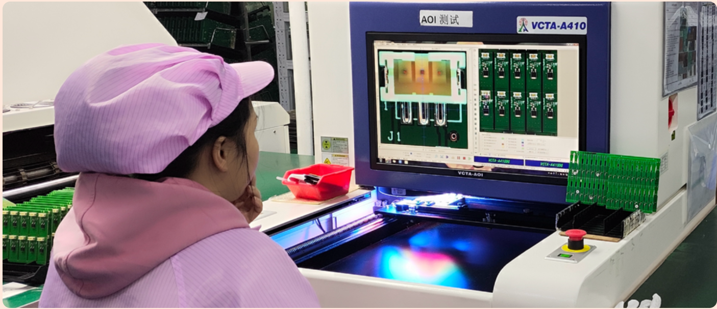
To meet quality assurance, large-scale PCB fabrication services adopt Automated Optical Inspection (AOI), In-circuit Test (ICT), Flying Probe Test and X-ray inspection. These commercial tests are used to locate printed circuit board fabrication defects through reliable inspection and testing techniques either through electrical method or non-electrical, non-contact methods.
Automated Optical Inspection
Automated Optical Inspection uses an image processing software to inspect a PCB by means of reference comparison method. The software has a defect detection algorithm to compare with a defect-free PCB. This helps PCB fabricators to detect defects and avoid hidden hazards. This is usually done by carrying out a pixel-to-pixel analysis and comparison to identify variation and locate the defects.
In-circuit Test
In-circuit test is the best testing method for high-volume PCB board fabrication. This testing method utilizes a fixture, also called bed-of-nails, to test the circuitry of the PCB. This type of PCB performance verification method is done in automatic mode, involving capacitance and resistance tests. ICT has efficient test throughputs and high test diagnostic accuracy and can provide quick feedback for short and open circuits.
Flying Probe Test
Flying probe testing is the most suitable testing method for small-scale production and prototyping as this testing is slower than ICT. This type of testing uses movable probes to contact the PCB test points and circuit pads. The movement of the probes is controlled through programming; thus this test has the advantage of testing high-density and complex circuitry due to its ability to access any contact point in the boards. Flying probe testing does not require a custom fixture, making it very cost-effective for small businesses.
Current and Future Trends of PCB Fabrication
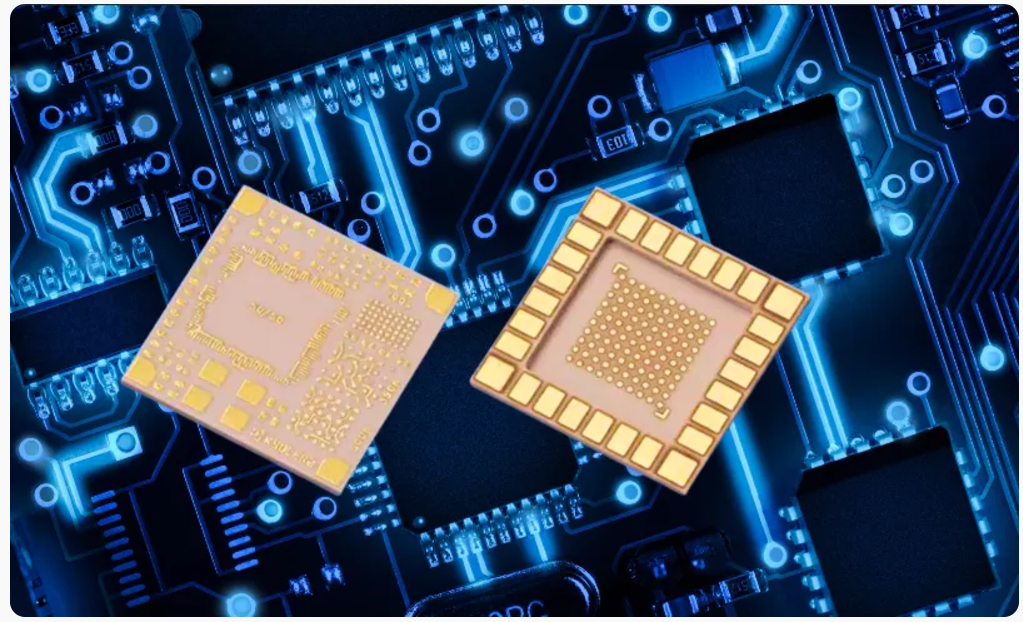
The future of printed circuit boards holds promising innovations and latest technologies to provide better functionality and efficiency. In recent years, research and industries have been studying 3D electronics, which allows direct printing of conductive traces on the device’s surfaces. This technology enables higher functionality and more complex designs while allowing space saving and weight reduction techniques.
Internet of Things (IoT) and Artificial Intelligence are also the major drivers in PCB fabrication technologies. The advancement of these areas made a breakthrough in mass production of electronic devices, allowing more data storage while miniaturizing the devices. Miniaturization drives further design improvements and manufacture of flexible PCBs and HDI circuitry.
The rise of automotive applications like ADAS (Advanced Driver Assistance System) and electronic vehicles will continuously affect PCB market when PCB fabricators try to fabricate PCB boards. ADAS requires better sensing systems for vehicles like lane assistance systems and passenger detection systems, thus increasing demands for electronics inside the cars.
Sustainability has also been taken into consideration when PCB fabricators prepare to fabricate PCBs. As environmental concerns are becoming more critical, recycling technologies are also constantly being studied. Government policies will also play a pivotal role in the market growth of printed circuit board fabrication by subsidizing expenditures, providing incentives, encouraging investments and focusing on research and development.
